Introduction
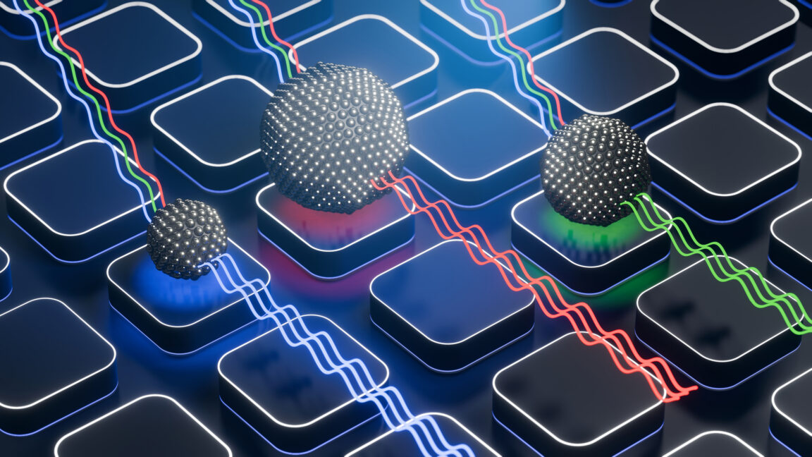
Quantum computing promises to revolutionize fields from cryptography to drug discovery, but it hinges on building large numbers of high-quality qubits that can be entangled arbitrarily. Two main approaches dominate: solid-state qubits embedded in manufactured electronics (scalable but fixed connectivity) and atomic or photonic qubits (flexible but hardware-intensive). A groundbreaking study now shows how to combine the best of both worlds using quantum dots — tiny semiconductor structures that can host a qubit as a single electron's spin. The key innovation? Moving these spin qubits between quantum dots without losing quantum information, enabling any-to-any connectivity akin to atomic systems. This guide walks you through the essential steps to manufacture and operate movable quantum dot qubits, from fabrication to verification.
What You Need
- Quantum dot array — A lithographically defined array of semiconductor quantum dots (e.g., on a GaAs/AlGaAs heterostructure) with tunable tunnel barriers.
- Control electronics — Voltage sources for gate electrodes (DC and fast pulsing) to manipulate electron confinement and tunneling.
- Cryogenic system — Dilution refrigerator capable of reaching temperatures below 100 mK to suppress thermal decoherence.
- Readout apparatus — Single-electron transistor (SET) or quantum point contact for charge detection and spin-to-charge conversion readout.
- Microwave electronics — For electron spin resonance (ESR) to manipulate spin states.
- Simulation software — For modeling electrostatic potentials and designing shuttling sequences.
Step-by-Step Guide
Step 1: Fabricate a Quantum Dot Array
Start by creating a linear or two-dimensional array of quantum dots using standard semiconductor nanofabrication techniques. Deposit metallic gate electrodes (e.g., Ti/Au) on a modulation-doped heterostructure to define depletion gates that form potential wells. Each quantum dot should be approximately 50–100 nm in diameter, with interdot spacing of 100–200 nm to allow tunneling. Ensure that gate voltages can independently control each dot's chemical potential and the tunnel barriers between them. See fabrication tips below.
Step 2: Isolate a Single Electron Spin Qubit
Cool the device to base temperature (below 100 mK) and apply gate voltages to confine exactly one electron in a chosen quantum dot. Verify the occupancy via charge sensing using a nearby SET. The electron's spin serves as the qubit. Use a magnetic field (typically 1–2 T) to split the spin states via Zeeman effect, enabling spin manipulation through electron spin resonance (ESR).
Step 3: Initialize and Characterize the Qubit
Initialize the qubit into a known spin state (e.g., spin-up) through spin-selective tunneling to a reservoir or via optical pumping. Characterize the qubit by performing Rabi oscillations — apply a resonant microwave pulse and measure the spin state as a function of pulse length. Extract the qubit frequency and coherence time $T_2^*$. Typical values for quantum dot spin qubits are $T_2^* \sim 1\text{–}10\,\mu\text{s}$.
Step 4: Prototype Coherent Shuttling
Design a voltage sequence that slowly (adiabatically) lowers the tunnel barrier between two adjacent quantum dots while simultaneously raising the barrier on the source dot, causing the electron to move to the target dot. The transfer must be adiabatic to avoid spin flips: the tunnel coupling should be much faster than the Zeeman energy (or the spin-orbit interaction). Use simulations to optimize pulse shapes. Implement the sequence using arbitrary waveform generators connected to the gate electrodes.
Step 5: Verify Qubit Fidelity After Movement
After shuttling the electron to the target dot, measure its spin state and compare to the initial state. Repeat with different distances (single dot, two dots, etc.) to quantify loss of quantum information. Key metrics: spin flip probability (should be below 1%) and coherence time retention. The landmark 2024 study demonstrated preservation of spin coherence over distances of several micrometers, with shuttling times of tens of nanoseconds.
Step 6: Scale to Multi-Dot Connectivity
Extend the shuttling protocol to move qubits across the entire array, enabling any two qubits to be brought into proximity for two-qubit gates (e.g., via exchange interaction). Develop calibration routines to compensate for disorder in the quantum dot potentials. Integrate error correction schemes that rely on flexible connectivity, such as the surface code, to achieve fault-tolerant logical qubits.
Tips and Best Practices
- Fabrication consistency: Ensure uniform dot sizes and tunnel barriers during lithography; even small deviations can disrupt shuttling.
- Noise mitigation: Use low-noise voltage sources and filter all lines to reduce charge noise, which degrades coherence.
- Adiabaticity: Shuttling speed must balance fast operation (to avoid decoherence) with slow enough changes to maintain spin state — typical ramp times of 10–100 ns work well.
- Spin-orbit coupling: In materials like InAs, strong spin-orbit interaction can cause spin flips during motion; choose GaAs or Si/SiGe for lower spin-orbit coupling.
- Readout optimization: Use radio-frequency reflectometry on SETs for fast, high-fidelity readout (>99%).
- Automated calibration: Implement machine learning algorithms to automatically tune gate voltages for optimal shuttling.
By following these steps and tips, you can create a platform that combines the scalability of manufactured qubits with the connectivity of atomic systems — a crucial milestone on the road to large-scale quantum computers.